


Description
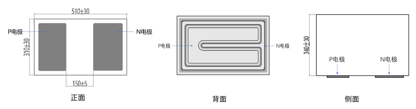
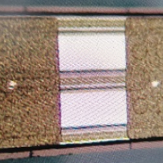
| Chip length | Chip width | Gap width | Chip thickness | Chip structure | electrode |
|---|---|---|---|---|---|
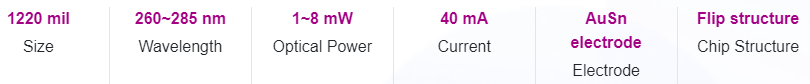
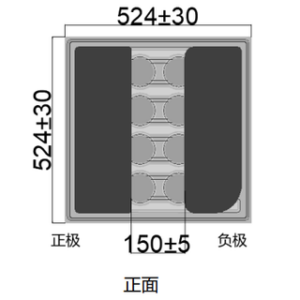
| 510±30 μm | 310±30 μm | 150±5 μm | 340±30 μm | Flip structure | AuSn electrode |
UVC photoelectric parameters and spec range (@ 40mA, Ta = 25 ℃, Rh = 30%)
| Item | Symbol | Min. | Typ. | Max. | Unit |
|---|---|---|---|---|---|
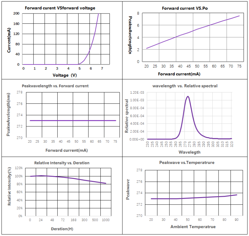
| Peak wavelength | λp | 260 | / | 285 | nm |
| Optical power | P0 | 1 | / | 8 | mW |
| working voltage | Vf | 5.0 | / | 7.5 | V |
| Driving current | If | / | 40 | / | mA |
| Maximum working current | Ifmax | / | / | 120 | mA |
| Maximum reverse bias | Ifmax | / | / | 0 | mA |
| FWHM of wave crest | Δλ | / | 11 | / | nm |
- The above specification range is subject to our measurement system. The measurement error of the measurement system is: peak wavelength( λp):±1nm; Optical power (P)0):±10%; Working voltage (V)f):±0.1V。
- Although all LEDs are tested by our equipment, some values may be slightly different depending on the conditions of the test equipment.
Wavelength range
| Groups | W01 | W02 | W03 |
|---|---|---|---|
| Wavelength (nm) | 260~270 | 270~280 | 280~285 |
Optical power range
| Groups | P01 | P03 |
|---|---|---|
| Optical power (MW) | 1~3 | 3~6 |
Voltage range
| Groups | V51 | V52 | V1B | V1C | V1D |
|---|---|---|---|---|---|
| Voltage (V) | 5.0~5.5 | 5.5~6.0 | 6.0~6.1 | 6.1~6.2 | 6.2~6.3 |
| Groups | V1E | V1F | V1G | V1H | V1I |
| Voltage (V) | 6.3~6.4 | 6.4~6.5 | 6.5~6.6 | 6.6~6.7 | 6.7~6.8 |
| Groups | V1J | V1K | V55 | ||
| Voltage (V) | 6.8~6.9 | 6.9~7.0 | 7.0~7.5 |
Environmental conditions for storage and use
| Item | Symbol | Unit | Value |
|---|---|---|---|
| Service temperature | TOPR | ℃ | -30 ~ +65 |
| Storage temperature | TSTG | ℃ | -40 ~ +85 |

- The above test data are from DUVTek, and the actual curve will be different depending on the sampling situation.

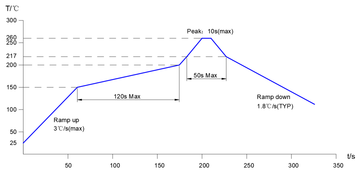
- The patch shall be reflow soldered with high temperature solder paste,The peak temperature should not be greater than 260 ℃The peak time should be controlled within 10 seconds and the reflux time should not be more than 5 minutes.
- Reflow welding should not be more than once;
- It is not recommended to repair after welding dark purple led. When repair is inevitable, double head soldering iron must be used, and the product itself should not be damaged while operating carefully;
- When welding, do not apply pressure on the deep UV LED during heating;
- It is recommended to use convection reflow welder with temperature above 7.
Label description
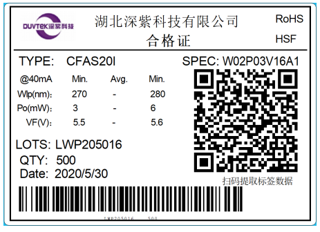
| label | interpretation |
|---|---|
| TYPE | Variety name |
| SPEC | For specification number, see the combination of various grading parameters |
| BIN No | Bin No |
| QTY | number |
| Date | date |
| Test items | experimental condition | standard | Failure ratio |
|---|---|---|---|
| Conventional drive | T = 25 ℃, calibration current, continuous lighting for 1000 hours | Dead lights | 0/35 |
| Thermal Shock | -40-120 ℃, 500 cycles, 15 min / cycle | Dead lights | 0/35 |
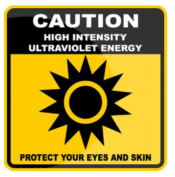
- All assembly workers, observers and bystanders must have eye and skin protection;
- It is forbidden to observe with naked eyes (including through microscope) and handle deep UV LED naked in operation;
- Do not touch the optical structure of the deep UV lamp bead;
- This product is a humidity sensitive product, the recommended storage temperature is 18 ℃~ 30 ℃, the humidity is 30% ~ 60%, and sealed. In order to ensure the product quality, it is recommended to use it within one year after leaving the factory if the outer packing bag is not opened; if the outer packing bag is opened, it is recommended to use it within 24 hours, and re seal it for storage after 24 hours. Dehumidification measures should be taken before the next use: temperature: 65 ℃ time: 5h.


Reviews
There are no reviews yet.